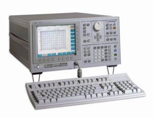
Agilent 4156C Semiconductor Parameter Analyzer
The 4156C is a precision semiconductor parameter analyzer designed for detailed electrical characterization of devices such as transistors, diodes, and advanced materials. It is part of Agilent Technologies’ classic parametric measurement line (now under Keysight Technologies), widely used in research labs and semiconductor development environments for DC and quasi-static measurements.
Key Features and Capabilities:
Precision DC Measurement Architecture:
Combines multiple high-resolution source/monitor units (SMUs) capable of sourcing and measuring voltage and current with sub-picoamp sensitivity. Enables accurate I–V characterization across a wide dynamic range.
Multi-Channel SMU Configuration:
Typically configured with 4 SMUs (expandable depending on modules), allowing simultaneous biasing and measurement of multi-terminal devices such as MOSFETs, BJTs, and compound semiconductor structures.
Ultra-Low Current Measurement:
Current resolution down to ~0.1 fA (model/config dependent), critical for leakage analysis, gate oxide characterization, and advanced node device research.
Wide Voltage and Current Ranges:
Supports sourcing from microvolts up to ±100 V and currents from femtoamps to tens of milliamps, covering both delicate nanoscale devices and higher-power discrete components.
Integrated Measurement Functions:
Built-in sweep capabilities (linear, logarithmic, pulsed-like quasi-static sweeps) for extracting key parameters such as threshold voltage, transconductance, subthreshold slope, and breakdown voltage.
Graphical Data Visualization & Analysis:
Onboard display provides real-time plotting of I–V curves and parametric sweeps, with cursor-based analysis tools for rapid extraction of device metrics.
Low Noise & Guarding Techniques:
Designed with triaxial connections and guarding to minimize leakage and noise, essential for ultra-low current and high-impedance measurements.
Programmability & Automation:
Supports GPIB and SCPI-based control for integration into automated test setups. Often used with external software for wafer probing and batch device characterization.
Scientific & Engineering Applications:
Semiconductor Device Characterization:
Extraction of MOSFET, BJT, and diode parameters including I–V curves, threshold voltage, leakage currents, and breakdown behavior.
Materials and Process Development:
Characterizing novel materials (e.g., wide bandgap semiconductors, 2D materials) and evaluating fabrication processes through electrical signatures.
Reliability & Failure Analysis:
Studying dielectric breakdown, hot carrier effects, and long-term device degradation through precise low-current measurements.
Wafer-Level Testing:
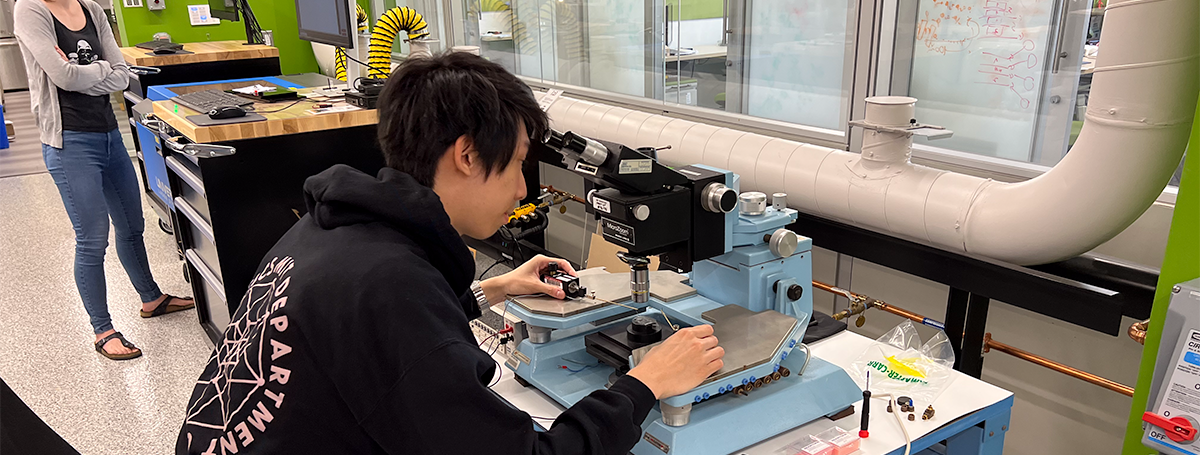
Integration with probe stations for automated testing of devices across wafers in R&D and low-volume production environments.
Sensor and Nanoelectronics Research:
Measuring ultra-low current devices such as MEMS sensors, photodetectors, and nanoscale transistors where leakage and noise are critical.
For more information:
- Ask Dr. Nagle
- Download the measurement and analysis manual
- Go to the manufacturer site