Past Engagements Portfolio
Steven F. Nagle, Ph.D.
Here I list publications and patents of mine, as well as related publications and patents. The related work is of note either because I had been deeply involved with it or I think it could be of value to an RLE researcher in a way that the Lab can help turn into practice.
Context: Once when trying to encourage me to take literature searches seriously, an MIT professor had told me that the quickest way to solve a problem was to already know the answer. We can decode that statement in many ways, but I have taken it to mean that most of any new body of work does not need to be reinvented. Only the truly unique crux(es) need be invented.
The scientific literature, even the patent record, contains many useful bits that the researcher can apply to all the hard work surrounding that crux. As you look through the body of work below, I hope that you find some useful bits. I also hope that you are encouraged to extend your literature searches, and other background research, to reserve your creativity for the crux.
Publications
2024 – Hu – Englund – Developing 3D Models of Atom-Like Defect Spin Memories in Crystals for Quantum Technology Research and Education
“The development of quantum technologies, including quantum computers and networks, requires entanglement distribution across individually controllable qubits. Color centers in diamond and silicon are leading solid-state qubits, so-called “artificial atoms”. Artificial atoms have been demonstrated for on-demand remote entanglement, coherent control of ancillary qubits with minute-long coherence times, and memory-enhanced quantum communication. There is an open need for clear and intuitive visualization of artificial atoms for research and education alike. Here we introduce a new visualization tool based on polyjet 3D printing technology to create detailed multimaterial multicolored 3D models of atomic defects, specifically focusing on color centers in diamond and silicon. These models accurately represent the defect structures in a hand-held form (less than 2 in.). We leverage the printer’s capability to deliver realistic patient-specific models with multiple materials on the same production run. This approach enhances quantum technology education by offering interactive tools and early introduction of quantum concepts in K-12, fostering a quantum-literate future generation.”
2022 – Borja – Dempsey – Highly Parallelized, Multicolor Optogenetic Recordings of Cellular Activity for Therapeutic Discovery Applications in Ion Channels and Disease-Associated Excitable Cells
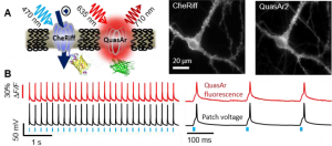
“Optogenetic assays provide a flexible, scalable, and information rich approach to probe compound effects for ion channel drug targets in both heterologous expression systems and associated disease relevant cell types. Despite the potential utility and growing adoption of optogenetics, there remains a critical need for compatible platform technologies with the speed, sensitivity, and throughput to enable their application to broader drug screening applications. To address this challenge, we developed the SwarmTM, a custom designed optical instrument for highly parallelized, multicolor measurements in excitable cells, simultaneously recording changes in voltage and calcium activities at high temporal resolution under optical stimulation. The compact design featuring high power LEDs, large numerical aperture optics, and fast photodiode detection enables all-optical individual well readout of 24-wells simultaneously from multi-well plates while maintaining sufficient temporal resolution to probe millisecond response dynamics. The Swarm delivers variable intensity bluelight optogenetic stimulation to enable membrane depolarization and red or lime-light excitation to enable fluorescence detection of the resulting changes in membrane potential or calcium levels, respectively. The Swarm can screen ∼10,000 wells/day in 384-well format, probing complex pharmacological interactions via a wide array of stimulation protocols. To evaluate the Swarm screening system, we optimized a series of heterologous optogenetic spiking HEK293 cell assays for several voltage-gated sodium channel subtypes including Nav1.2, Nav1.5, and Nav1.7. The Swarm was able to record pseudo-action potentials stably across all 24 objectives and provided pharmacological characterization of diverse sodium channel blockers. We performed a Nav1.7 screen of 200,000 small molecules in a 384-well plate format with all 560 plates reaching a Z′ > 0.5. As a demonstration of the versatility of the Swarm, we also developed an assay measuring cardiac action potential and calcium waveform properties simultaneously under paced conditions using human induced pluripotent stem (iPS) cell-derived cardiomyocytes as an additional counter screen for cardiac toxicity. In summary, the Swarm is a novel high-throughput all-optical system capable of collecting information-dense data from optogenetic assays in both heterologous and iPS cell-derived models, which can be leveraged to drive diverse therapeutic discovery programs for nervous system disorders and other disease areas involving excitable cells.”
2017 – Werley – Wasserman – An ultra-widefield microscope for high-speed, all-optical electrophysiology
“Using optogenetics, the ultrawidefield Firefly microscope enables simultaneous stimulation with blue light and transmembrane voltage recordings with red light from >100 neurons with subcellular spatial and millisecond temporal resolution.”
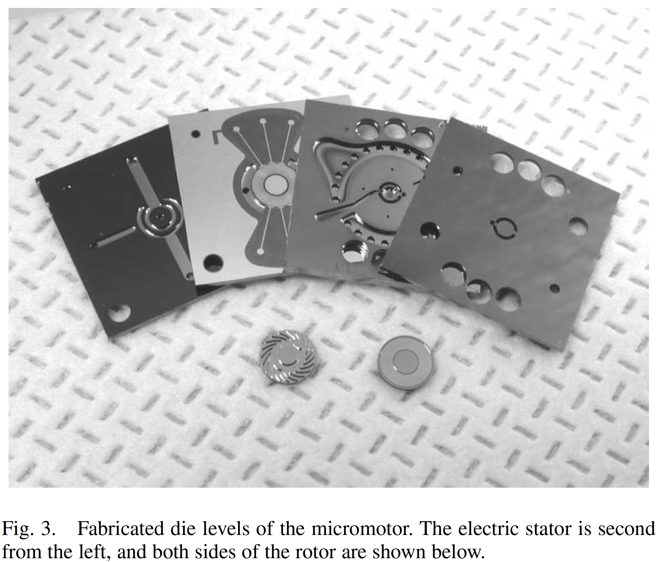
2005 – Nagle – Lang – An Electric Induction Micromotor
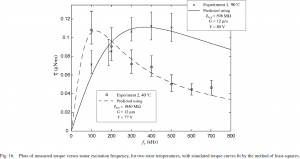
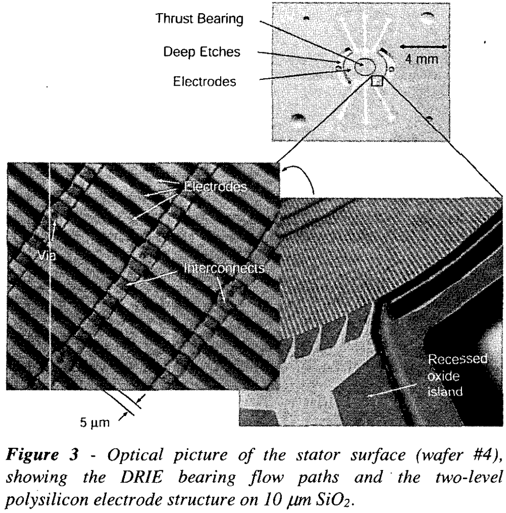
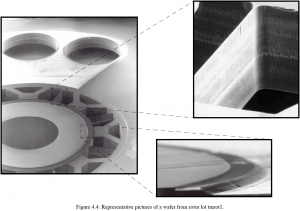
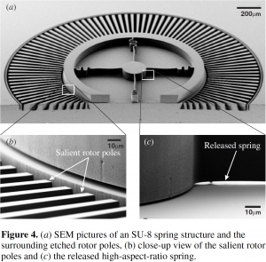
“This paper presents the analysis, design, fabrication, and testing of a planar electric induction micromotor. The micromotor is a 6-phase motor with 131 pole pairs distributed on a stator having a 4 mm outer diameter. The axial air gap is 3 μm. With a 90 V stator excitation, applied at a 300 kHz slip frequency, the motor produces a torque of 2 μN-m. Special attention is paid to the limitations that microfabrication places on the design of the motor.”
2003 – Ayon – Spearing – Characterization of silicon wafer bonding for Power MEMS applications
“This paper reports the investigation of low-temperature silicon wafer fusion bonding for MEMS applications. A bonding process utilizing annealing temperatures between 400 and 1100 C was characterized. The silicon–silicon bonded interface was analyzed by infrared transmission (IT) and transmission electron microscopy (TEM) and the bond toughness was quantified by a four-point bending-delamination technique.”
2001 – Frechette – Lang – An electrostatic induction micromotor supported on gas-lubricated bearings
“This paper reports the first successful fabrication and demonstration of an electrostatic induction micromotor supported on gas-lubricated bearings for electrical-to-mechanical energy conversion. The device consists of a stack of five (5) deep reactive ion etched (DRIE) fusion bonded silicon wafers, with an enclosed 4.2 mm diameter rotor driven by a high-voltage, high-frequency thin-film stator. Testing has demonstrated a torque of 0.3 μN-m at a rotation rate of 15,000 revolutions per minute, corresponding to a shaft power of 0.5 mW. This development effort serves to support the creation of a wide array of power MEMS devices such as micro-scale pumps, compressors, generators, and coolers.”
2001 – Nagle – Analysis, Design, and Fabrication of an Electric Induction Micromotor for a Micro Gas-Turbine Generator
(see also: 2005 – Nagle – Lang – An Electric Induction Micromotor)
“This thesis presents the analysis, design, fabrication, and testing of the first axial-gap electric induction micromotor, and the first controlled measurement of electric micromotor torque using integrated mechanical springs. Electric induction micromotors offer several advantages over electric variable capacitance micromotors and magnetic micromotors: neither rotor position nor speed need be known to achieve good performance; perfect sinusoids can be used for actuation to eliminate switching losses without loss of motor performance. In addition, the motor is fabricated from IC-compatible materials. …
Torque is measured as high as 0.220 μN-m with 90 V square-wave actuation. Torque is shown to be consistent with models and the torque curves are shown to shift with rotor conductivity as expected with reference to a magnetic induction machine. The measurements are consistent with a gap of 12 μm, which is shown to be a result of the hand-assembly process. Bonding would yield a gap of 3 μm, making torque of 3 μN-m possible at the same voltage.”
1999 – Ayon – Schmidt – Characterization of a Time Multiplexed Inductively Coupled Plasma Etcher
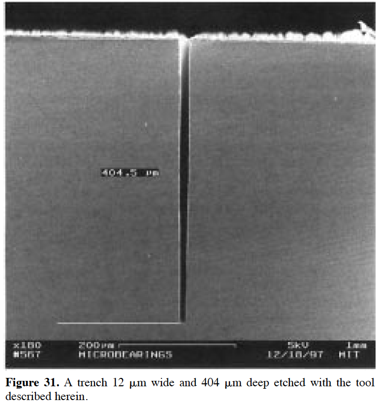
“We report the experimentally obtained response surfaces of silicon etching rate, aspect ratio dependent etching (ARDE), photoresist etching rate, and anisotropy parameter in a time multiplexed inductively coupled plasma etcher. The data were collected while varying eight etching variables. The relevance of electrode power, pressure, and gas flow rates is presented and has been found to agree with observations reported in the literature. The observed behavior presented in this report serves as a tool to locate and optimize operating conditions to etch high aspect ratio structures. The performance of this deep reactive ion etcher allows the tailoring of silicon etching rates in excess of 4 μm/min with anisotropic profiles, nonuniformities of less than 4% across the wafer, and ARDE control with a depth variation of less than 1 μm for trenches of dissimilar width. Furthermore it is possible to prescribe the slope of etched trenches from positive to reentrant. …
Figure 31. A trench 12 μm wide and 404 μm deep etched with the tool described herein.”
1997 – Epstein – Waitz – Power MEMS and microengines
“MIT is developing a MEMS-based gas turbine generator. Based on high speed rotating machinery, this 1 cm diameter by 3 mm thick SiC heat engine is designed to produce 10-20 W of electric power while consuming 10 grams/hr of H<sub>2</sub>. Later versions may produce up to 100 W using hydrocarbon fuels. The combustor is now operating and an 80 W micro-turbine has been fabricated and is being tested. This engine can be considered the first of a new class of MEMS device, power MEMS, which are heat engines operating at power densities similar to those of the best large scale devices made today.”
1996 – Nagle – Lakhtakia – Shear axial modes in a PCTSCM Part II- towards transduction applications
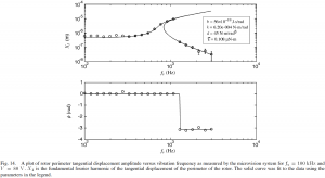
“Electrically excited axial shear wave propagation within a piezoelectric continuously twisted structurally chiral medium (PCTSCM) plate is examined. Three different plates with distinct material properties are considered, each plate operating in one of three zone.s in spatiotemporal space. The excited field in each plate is examined by plotting the local polarization angle, the total shear displacement field amplitude, as well as the total field along the helicoidal axis of the PCTSCM. Although the local vibration ellipse of every individual mode rotates in conformity with the material structure, the total field does not. Individual modes beat with each other to produce distinct field behavior in each plate. As modal wavelengths do not scale in proportion to the helicoidal pitch of any of the three plates, axial propagation behavior turns out to be unique in each plate.”
1995 – Nagle – Lakhtakia – Shear axial modes in a PCTSCM Part I- piezoelectric stiffening and selective attenuation
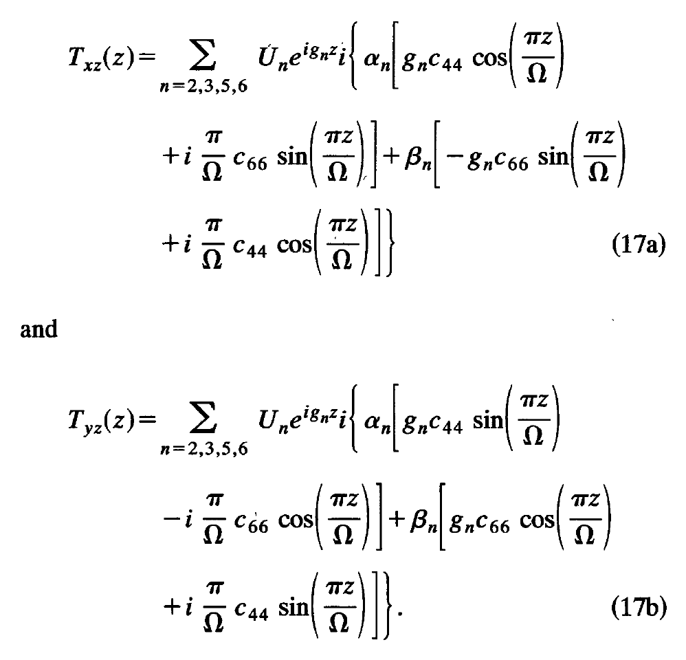
“The material properties of a piezoelectric continuously twisted structurally chiral medium (PCTSCM) vary helicoidally along the axial direction. Since the degree of piezoelectric coupling can be engineered to a reasonable extent, PCTSCMs are promising candidates for future transduction devices. In this paper, we implement the quasi-electrostatic approximation for axial propagation modes in PCTSCMs, particularly for those with hexagonal 6mm reference crystal symmetry. Axial propagation of shear modes is affected by piezoeletric stiffening. Axial propagation displays selective attenuation and can be classified into three zones. The zone of selective attenuation can be altered by the degree of piezoelectric stiffening as well as by the spatial frequency of the PCTSCM.”
1994 – Nagle – Thompson – Modal structures for axial wave propagation in a continuously twisted structurally chiral medium
“The stiffness of a continuously twisted structurally chiral medium (CTSCM) varies helicoidally about the axis of spirality. The structures of axial propagation modes in a CTSCM having a tetragonal reference symmetry have been investigated in this paper. Salient features relating to the management of the phase and the vibration ellipse have been brought out, and may be of assistance in conceptualizing novel devices with plane-stratified geometries. …
Devices based on the wave concept and with plane stratified geometries involve skillful management of the amplitude, the phase and the vibration ellipse. Such devices include transducers of various kinds, polarizers, absorbers, etc. We have shown from our analysis that the axial shear modes in a CTSCM offer many different avenues for managing the phase and the vibration ellipse; thus their potential for actuating, sensing, polarizing, and beamforming has been established.”
1994 – Nagle – Lakhtakia – Attenuation and handedness of axial propagation modes in a cholesteric liquid crystal
“The interplay of spatial and temporal periodicities in a cholesteric liquid crystal is responsible for the three zones into which axial propagation may be classified. Each of the three zones is marked by specific attenuation and handedness characteristics. …
We note a previously unrecognized general result that Fn is not a function of z for axial propagation in any helicoidally bianisotropic medium. …”
Select Related Publications
2011 – Kuhne – Hierold – Fabrication and characterization of a tethered rotational planar variable capacitance micro drive
“In this paper, we present the design, fabrication and characterization of a planar variable capacitance micro drive. The rotational micro drive is developed for high-speed applications with contactless active electrostatic micro bearings. The associated low-temperature process allows the fabrication of devices with narrow stator–rotor gaps. The drive performance is characterized by means of tethered functional prototype devices. The multicompliant devices have silicon rotors and a soft polymer suspension, which allows the validated modeling of the drive capacitance and accurate measurement of the static drive torques. The devices achieve up to 2.6 nNm static drive torque per phase at an actuation voltage of 12 V. These results demonstrate the highest torque generation of a planar variable capacitance drive at low actuation voltages.”
2010 – Liu – Yeo – A brief review of actuation at the micro-scale using electrostatics, electromagnetics and piezoelectric ultrasonics
“Though miniaturization and mass production via integrated circuit fabrication techniques have transformed our society, the methods have yet to be successfully applied to the generation of motion, and as a consequence the many potential benefits of microrobotics has yet to be realized. The characteristics of electrostatic, electromagnetic and piezoelectric transduction for generating motion at the micro scale is considered, employing scaling laws and a reasoned consideration of the difficulties in motor fabrication and design using each method. The scaling analyses show that electrostatic, electromagnetic and piezoelectric actuators all have comparable force scaling characteristics of F ∝ L2; if one employs permanent magnets, electromagnetic forces do not scale as F ∝ L4. Though the torque, τ, of piezoelectric ultrasonic motors scale rather poorly with τ ∝ L4, they have the clear advantage of possessing torque amplitudes some two orders of magnitude larger than motors employing the other transduction schemes at the micro scale.”
2009 – Steyn – Livermore – A Self-Excited MEMS Electro-Quasi-Static Induction Turbine Generator
“This paper presents a microfabricated electro-quasistatic (EQS) induction turbine generator that has generated net electric power. A maximum power output of 192 μW was achieved under driven excitation. We believe that this is the first report of net-electric-power generation by an EQS induction machine of any scale found in the open literature. This paper also presents self-excited operation in which the generator resonates with an inductor and generates power without the use of external active-drive electronics. The generator comprises five silicon layers, fusion-bonded together at 700 ◦C. The stator is a platinum electrode structure formed on a thick (approximately 20 μm) recessed oxide island. The rotor is a thin film of lightly doped polysilicon also residing on a 10-μm-thick oxide island. Carrier depletion in the rotor conductor film limited the performance of the generator. This paper also presents a generalized state-space model for an EQS induction machine that takes into account the machine and its external electronics and parasitics. This model correlates well with measured performance and was used to find the optimal drive conditions for all driven experiments.”
2004 – Livermore – Lang – A High-Power MEMS Electric Induction Motor
“An electric induction micromotor with a 4-mm-diameter rotor was designed and built for high-power operation. Operated at partial actuating voltage, the motor has demonstrated an air gap power in excess of 20 mW and torque of 3.5 μN-m at speeds in excess of 55,000 rpm. Operation at higher power and speed was limited by bearing stability at higher rotational speeds. The device builds on an earlier micromotor demonstrated by Frechette et al. The high power of the present motor is enabled by its low-loss, high-voltage electric stator, which also offers improved efficiency. The development of this electromechanical device is an important enabling step not only for watt-scale micromotors, but also for the development of microelectric generators. This paper presents the motor’s design, the fabrication process that was created to meet its stringent design requirements, and its performance to date.”
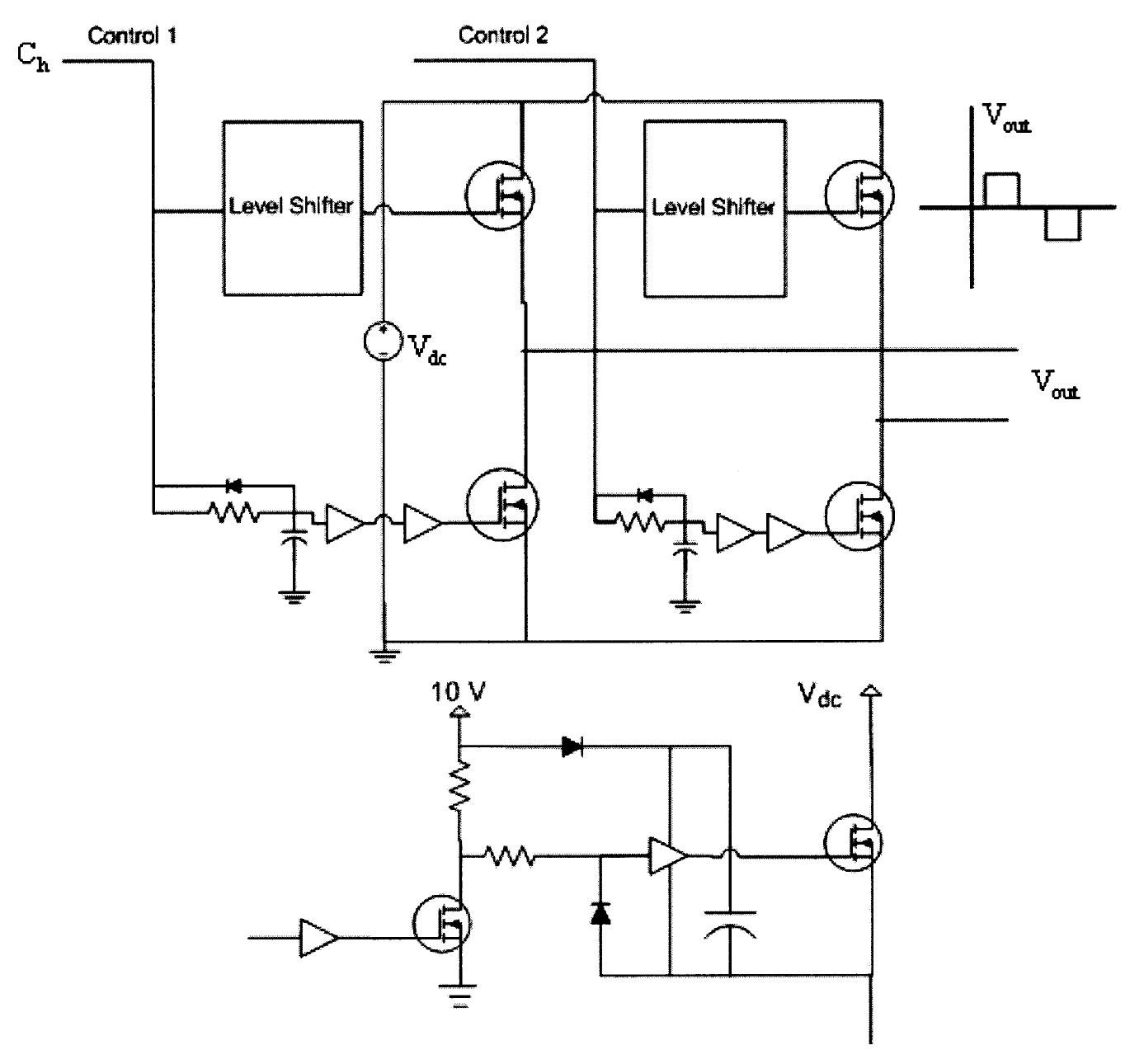
2004 – Neubquer – Livermore – A Six-Phase Multilevel Inverter for MEMS Electrostatic Induction Micromotors
“The construction of miniaturized rotating electric machines through microfabrication techniques is becoming a reality. Applications of such micromotors include miniaturized pumps, compressors, fans, coolers, and turbogenerators. However, the characteristics of these devices make the design of power electronics for them challenging. These characteristics include high-voltage and high-frequency operation, tightly constrained operating waveforms and timing, and capacitive input impedances. This paper explores the design of power electronics for microfabricated electrostatic induction machines. We describe the structure and operation of these machines, and establish the operating requirements of power converters for them. We provide a comparison of inverter topologies for this application, and propose an appropriate architecture. The design and experimental evaluation of a prototype six-phase, five-level inverter for this application is presented. The inverter operates at frequencies up to 2 MHz and at voltages up to 300 V, and meets the stringent waveform and timing constraints posed by this application.”
Inventions
US11931737 PLATFORMS AND SYSTEMS FOR AUTOMATED CELL CULTURE
“Disclosed herein are platforms, systems, and methods including a cell culture system that includes a cell culture container comprising a cell culture, the cell culture receiving input cells, a cell imaging subsystem configured to acquire images of the cell culture, a computing subsystem configured to perform a cell culture process on the cell culture according to the images acquired by the cell imaging subsystem, and a cell editing subsystem configured to edit the cell culture to produce output cell products according to the cell culture process.”
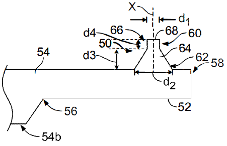
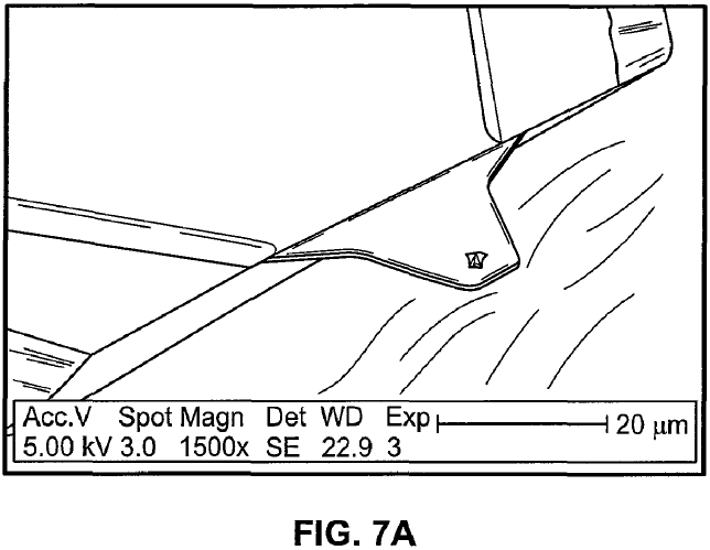
US8595860 METHOD OF FABRICATING A PROBE DEVICE FOR A METROLOGY INSTRUMENT AND A PROBE DEVICE PRODUCED THEREBY
“A method of producing a probe device for a metrology instrument such as an AFM includes providing a substrate and forming a tip stock extending upwardly from the substrate. The tip stock is preferably FIB milled to form a tip of the probe device. The tip preferably has a high aspect ratio, with a height that is at least about 1 micron for performing critical dimension (e.g., deep trench) atomic force microscopy. The stock is preferably pedestal shaped having a distal end that is substantially planar which can be machined into a tip in at least less than about 2 minutes. With the preferred embodiments, the FIB milling step can be completed in substantially fewer and less complicated steps than known techniques to produce a high aspect ratio tip suitable for DT-AFM in less than about one minute.”
US7823216 PROBE DEVICE FOR A METROLOGY INSTRUMENT AND METHOD OF FABRICATING THE SAME
“A method of producing a probe device for a metrology instrument such as an AFM includes providing a substrate having front and back surfaces and then forming an array of tip height structures on the first surface of the substrate, the structures having varying depths corresponding to selectable tip heights. The back surface of the substrate is etched until a thickness of the substrate substantially corresponds to a selected tip height, preferably by monitoring this etch visually and/or monitoring the etch rate. The tips are patterned from the front side of the wafer relative to fixed ends of the cantilevers, and then etched using an anisotropic etch. As a result, probe devices having sharp tips and short cantilevers exhibit fundamental resonant frequencies greater than 700 kHz or more.”
US7770231 FAST-SCANNING SPM AND METHOD OF OPERATING SAME
“A method and apparatus are provided that have the capability of rapidly scanning a large sample of arbitrary characteristics under force control feedback so as to obtain a high resolution image. The method includes generating relative scanning movement between a probe of the SPM and a sample to scan the probe through a scan range of at least 4 microns at a rate of at least 30 lines/sec and controlling probe-sample interaction with a force control slew rate of at least 1 mm/sec. A preferred SPM capable of achieving these results has a force controller having a force control bandwidth of at least closed loop bandwidth of at least 10 kHz.”
US7208333 PROCESS FOR FABRICATING MEMS MEMBRANE WITH INTEGRAL MIRROR/LENS
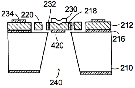
“An optical membrane device and method for making such a device are described. This membrane is notable in that it comprises an optically curved surface. In some embodiments, this curved optical surface is optically concave and coated, for example, with a highly reflecting (HR) coating to create a curved mirror. In other embodiments, the optical surface is optically convex and coated with, preferably, an antireflective (AR) coating to function as a refractive or diffractive lens.”
US6768756 MEMS MEMBRANE WITH INTEGRAL MIRROR/LENS
“An optical membrane device and method for making such a device are described. This membrane is notable in that it comprises an optically curved surface. In some embodiments, this curved optical surface is optically concave and coated, for example, with a highly reflecting (HR) coating to create a curved mirror. In other embodiments, the optical surface is optically convex and coated with, preferably, an antireflective (AR) coating to function as a refractive or diffractive lens.”
US6643075 REENTRANT-WALLED OPTICAL SYSTEM TEMPLATE AND PROCESS FOR OPTICAL SYSTEM FABRICATION USING SAME
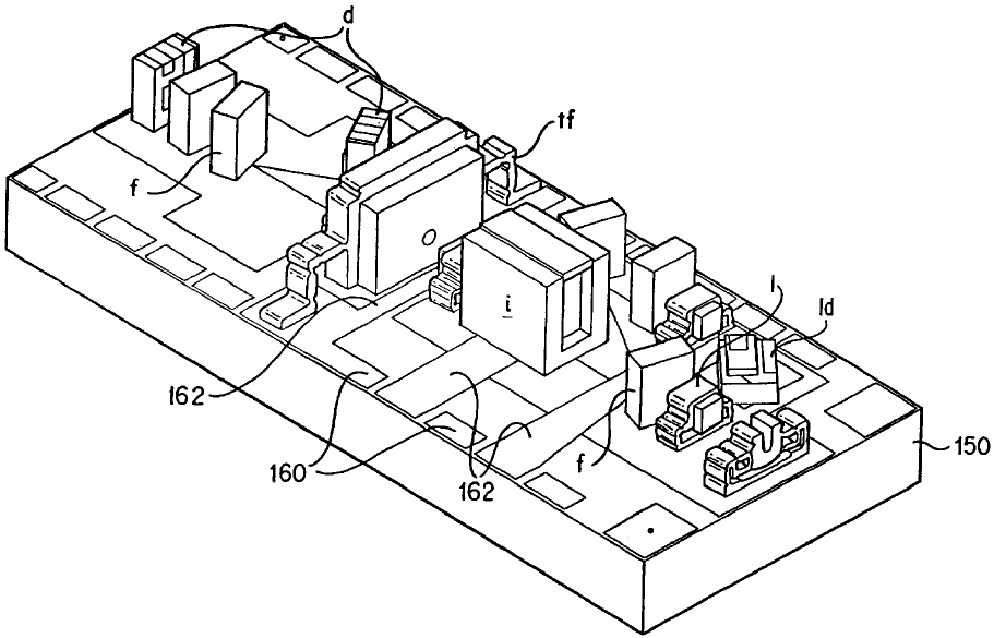
“An optical system assembly technique utilizes a templating system for location optical components 200 on optical benches 150. Specifically, the template system comprises a template substrate 102 that is placed over the optical bench. The substrate 102 has at least one alignment slot 104 that is formed through the substrate. This alignment slot 104 has an alignment feature 120, against which an optical component 200 is registered. In order to improve the accuracy of the alignment of the optical component on the optical bench, the slot 104 has a reentrant, such as a smooth or step, sidewall 106 extending from the alignment feature 120 into the template substrate 102. This way, there is a single point or near single point of contact between the optical component 200 and the template 102, to thereby improve the placement precision for the optical component on the optical bench 150.“
US6392313 MICROTURBOMACHINERY
“The invention overcomes limitations of conventional power and thermodynamic Sources by with micromachinery components that enable production of Significant power and efficient operation of thermodynamic Systems in the milli meter and micron regime to meet the efficiency, mobility, modularity, weight, and cost requirements of many modern applications. A micromachine of the invention has a rotor disk journaled for rotation in a Stationary Structure by a journal bearing. A plurality of radial flow rotor blades, Substantially untapered in height, are disposed on a first rotor disk face, and an electrically conducting region is disposed on a rotor disk face. A plurality of Stator electrodes that are electrically interconnected to define multiple electrical Stator phases are disposed on a wall of the Stationary Structure located opposite the electrically conducting region of the rotor disk. A first orifice in the Stationary Structure provides fluidic communication with the first rotor disk face at a location radially central of the rotor blades, and a Second orifice in the Stationary Structure provides fluidic communication with the first rotor disk face at a location radially peripheral of the rotor blades. An electrical connection to the Stator electrode configuration is provided for Stator electrode excitation and for power transfer with the Stator electrode configuration as the rotor disk rotates.”
Select Related Inventions
US6385382 ALIGNMENT SYSTEM OPTICAL COMPONENT INTERFACE
“A mechanical interface between a manipulation system and an optical component in which manipulation system jaws are adapted to engage an optical component at a handle and then deform the component. In some applications, an optical component is translationally or rotationally deformed. In one example, the jaws are moved towards each other in an opposed fashion such that teeth engage the optical component at the handle. Then, the jaws are collectively actuated so that they are moved in substantially the same direction. This results, typically, in the deformation of the optical component so that the optical element held by the optical mounting structure is moved into an improved alignment position. In another example, a V-shaped slot in one of the jaws is used to grasp the optical element, e.g., fiber, to move the element.”


